- 您现在的位置:买卖IC网 > Sheet目录1996 > HSP45106JC-33Z (Intersil)IC OSC NCO 33MHZ 84-PLCC
2
FN2809.8
October 16, 2008
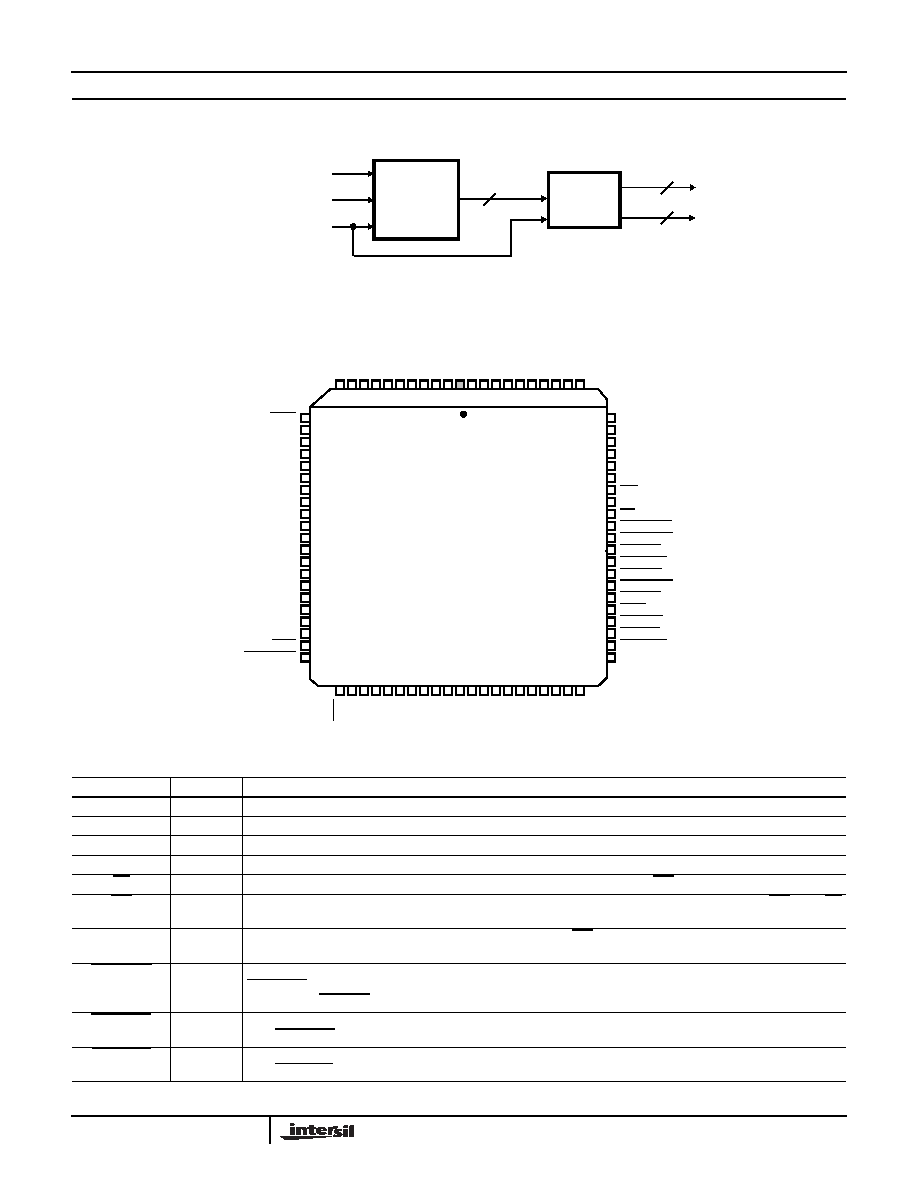
Block Diagram
PHASE/
FREQUENCY
CONTROL
SECTION
SINE/
COSINE
SECTION
SINE
COSINE
CLOCK
MICROPROCESSOR
INTERFACE
DISCRETE
CONTROL SIGNALS
32
16
SIN/COS
ARGUMENT
Pinouts
HSP45106
(84 LD PLCC)
TOP VIEW
Pin Descriptions
NAME
TYPE
DESCRIPTION
VCC
+5 power supply pin.
GND
Ground.
C(15:0)
I
Control input bus for loading phase, frequency, and timer data into the PFCS. C0 is LSB.
A(2:0)
I
Address pins for selecting destination of C(15:0) data (Table 2). A0 is the LSB
CS
I
Chip select (active low). Enables data to be written into Control Registers by WR.
WR
I
Write enable (active low). Data is clocked into the register selected by A(2:0) on the rising edge of WR when CS
is low.
CLK
I
Clock. All registers, except the Control Registers clocked with WR, are clocked (when enabled) by the rising edge
of CLK.
ENPOREG
I
Phase Offset Register Enable (active low). Registered on chip by CLK. When active, after being clocked onto chip,
ENPOREG enables the clocking of data into the Phase Offset Register. Allows ROM address to be updated
regardless of ENPHAC.
ENOFREG
I
Offset Frequency Register Enable (active low). Registered on chip by CLK. When active, after being clocked onto
chip, ENOFREG enables the clocking of data into the Offset Frequency Register.
ENCFREG
I
Center Frequency Register Enable (active low). Registered on chip by CLK. When active, after being clocked onto
chip, ENCFREG enables the clocking of data into the Center Frequency Register.
GND
CLK
SI
N0
SI
N1
SI
N2
SI
N3
SI
N4
V
CC
SI
N5
SI
N6
SI
N7
SI
N8
SI
N9
SI
N
1
0
SI
N1
1
SI
N
1
2
GND
SI
N
1
3
SI
N
1
4
SI
N
1
5
OES
11 10 98 765 432 1 84 83 82 81 80 79 78 77 76 75
12
13
14
15
16
17
18
19
20
21
22
23
24
25
26
27
28
29
30
31
32
33 34 35 36 37 38 39 40 41 42 43 44 45 46 47 48 49 50 51 52 53
74
73
72
71
70
69
68
67
66
65
64
63
62
61
60
59
58
57
56
55
54
TICO
COS15
COS14
COS13
GND
COS12
COS11
COS10
COS9
COS8
COS7
COS6
COS5
COS4
VCC
COS3
COS2
COS1
COS0
OEC
DACSTRB
PMSEL
MOD0
MOD1
MOD2
TEST
VCC
WR
GND
CS
ENCFREG
ENOFREG
INHOFR
ENTIREG
INITTAC
ENPOREG
INPHAC
PACI
INITPAC
BINFMT
PAR/SER
VCC
C0
C1
C2
C3
C4
C5
C6
V
CC
C7
C8
C9
C10
C1
1
C12
C13
C14
C15
GN
D
A0
A1
A2
HSP45106
发布紧急采购,3分钟左右您将得到回复。
相关PDF资料
HSP45116AVC-52Z
IC OSC NCO 52MHZ 160-MQFP
ICL7109EPL+
IC ADC 12BIT 3-ST 40-DIP
ICM7217AIPI
IC OSC UP/DWN CNTR 2MHZ 28-DIP
ICM7217CIPI
IC OSC UP/DWN CNTR 2MHZ 28-DIP
ICM7242IPA
IC OSC BINARY CTC 13MHZ 8-DIP
ICM7250IWE+T
IC OSC BINARY CTC 15MHZ 16SOIC
ICM7556IPD
IC OSC TIMER DUAL 500KHZ 14-DIP
ICM7556MJD
IC OSC TIMER DUAL 1MHZ 14DIP
相关代理商/技术参数
HSP45106JI-25
制造商:Rochester Electronics LLC 功能描述:- Bulk
HSP45116
制造商:INTERSIL 制造商全称:Intersil Corporation 功能描述:Numerically Controlled Oscillator/Modulator
HSP45116 WAF
制造商:Intersil Corporation 功能描述:
HSP45116/883
制造商:INTERSIL 制造商全称:Intersil Corporation 功能描述:Numerically Controlled Oscillator/Modulator
HSP45116_04
制造商:INTERSIL 制造商全称:Intersil Corporation 功能描述:Numerically Controlled Oscillator/Modulator
HSP45116883
制造商:INTERSIL 制造商全称:Intersil Corporation 功能描述:Numerically Controlled Oscillator/Modulator
HSP45116A
制造商:INTERSIL 制造商全称:Intersil Corporation 功能描述:Numerically Controlled Oscillator/Modulator
HSP45116A_07
制造商:INTERSIL 制造商全称:Intersil Corporation 功能描述:Numerically Controlled Oscillator/Modulator